
Nanofabrication
Lithography technology
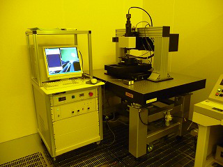
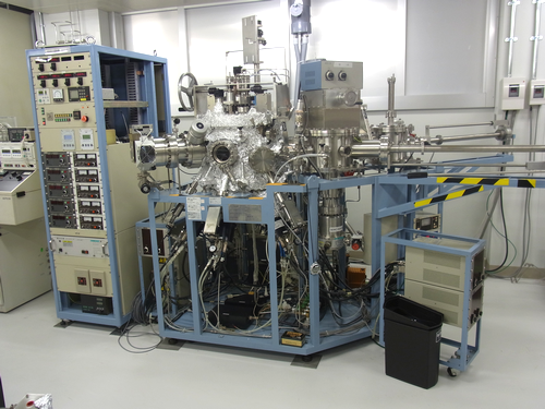
ELS-F125 Ultra-high precision electron-beam lithography system (Elionix)
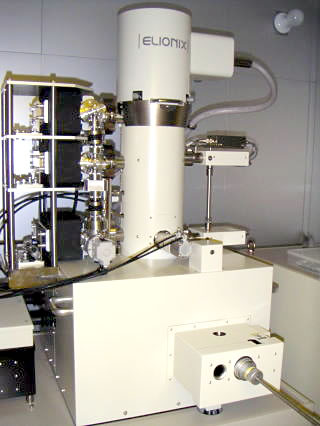
Specifications
・Electron gun emitter: ZrO/W thermal field emitter
・Acceleration voltage: 125, 75, 25 kV
・Minimum line width: 5 nm (125 kV)
・Maximum specimen size: 6 inches
Characteristics
Electron beam allows nano-level fine pattern writing (minimum line width: 5 nm) on resist materials and other media
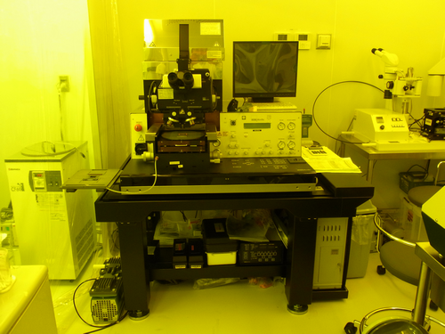
ELS-7000HM Ultra-high precision electron-beam lithography system (Elionix)
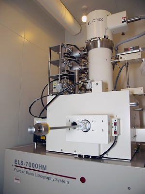
Specifications
・Electron gun emitter: ZrO/W
・Thermal field emission-type acceleration voltage: 25, 50, 75, 100 kV
・Minimum line width: 8 nm (5 nm-compatible)
・Maximum specimen size: 6 inches
Characteristics
Electron beam allows nano-level fine pattern writing (minimum line width: 8 nm) on resist materials and other media
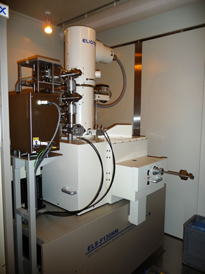
ELS-3700 Electron-beam lithography system (Elionix)
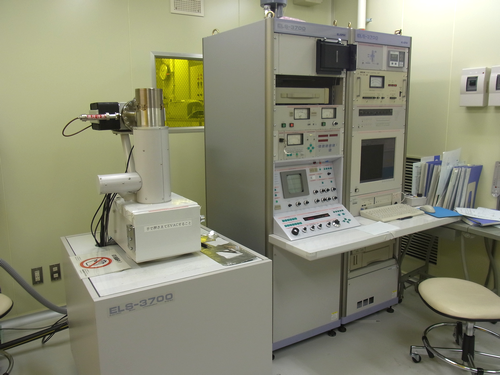
Specifications
・Electron gun emitter: LaB6
・Acceleration voltage: 1 to 30 kV
・Minimum line width: 100 nm
・Maximum specimen size: 4 inches
・Arc-scannable
Characteristics
Exposure device for direct electron-beam writing on resist materials applied to substrates
ELS-7300 Electron-beam lithography system (Elionix)
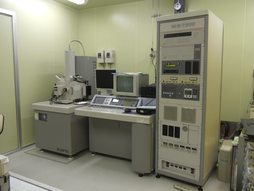
Specifications
・Electron gun emitter: ZrO/W
・Acceleration voltage: 30 kV
・Maximum specimen size: 5 inches
・Arc-scannable
Characteristics
Exposure device for direct electron-beam writing on resist materials applied to substrates
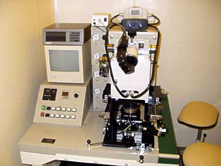
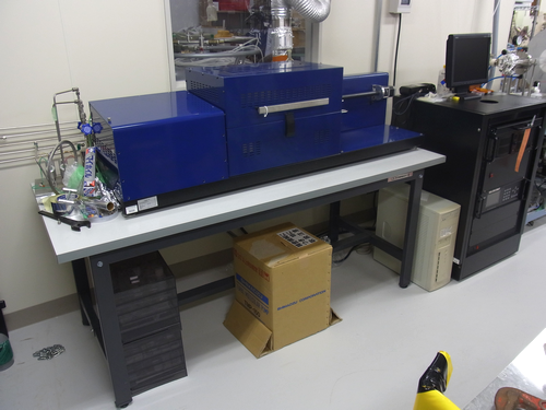
DDB-201 Laser direct lithography system (Neoark)
Specifications
・Light source: 375-nm semiconductor laser
・Maximum writing area: 50 mm
・Maximum specimen size: 6 inches
・Minimum line width: 1 μm
Characteristics
Exposure device for direct laser-beam writing in micron order on resist materials applied to substrates
MA-6 Double-side mask aligner (Suss MicroTec)
Specifications
・Double-sided; exposure accuracy: 0.6 microns
・Maximum specimen size: 6 inches
・Substrate size: pieces of undefined size to 150 × 150 mm
Characteristics
High-performance double-side manual mask alignment adaptable to thick resists
MA-20 Mask aligner (Mikasa)
Specifications
・Contact exposure
・Maximum specimen size: 4 inches
・Maximum mask size: 5 inches
Characteristics
Exposure device with highly uniform illumination distribution characteristics and a multi-mirror lamp house as the light source
Ultra high speed scanning and high precision electron beam lithography system
Specifications
・Electron gun emitter: ZrO/W thermal field emitter
・Acceleration voltage:130kV
・Maximum specimen size:8 inches
Characteristics
Advanced clock frequency allows you to draw faster than ELS-F125
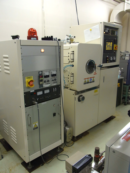
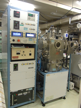
Film formation technology
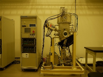
ED-1500R Vacuum deposition system (Sanvac)
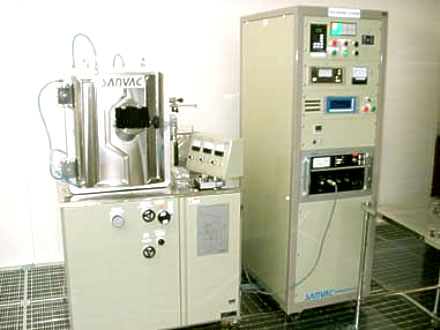
Specifications
・Deposition sources: resistance heating × 3, EB × 3
・Suitable for substrate heating
・Crystal oscillation-type film thickness meter
Characteristics
Vacuum deposition system with three evaporation sources and an electron gun for deposition of metals, semiconductors and inorganic insulators. Capable of forming multilayer deposition film.
EBX-8C EB heating/resistant heating-type deposition system (Ulvac)
Specifications
・Deposition sources: EB × 4, resistance heating × 2
・Deposition materials: Ti, Au, Al, Pd, Co, others
Characteristics
Deposition system capable of forming electrode film and insulating thin film on the surface of substrates, thin film samples and other materials through heat transpiration of metals or semiconductor compounds in a vacuum
EB heating/resistant heating-type deposition system (Suga)
Specifications
・Deposition sources: EB × 4, resistance heating × 1
・Deposition materials: Si, Al, Fe, Mo, Au
Characteristics
Deposition system capable of forming electrode film and insulating thin film on the surface of substrates, thin film samples and other materials through heat transpiration of metals or semiconductor compounds in a vacuum
PD-220ESN Plasma CVD system (Samco)
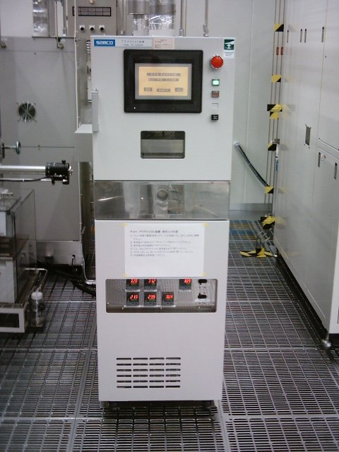
Specifications
・Specimen types: SiO2, SiN
・Maximum specimen size: 4 inch wafer
Characteristics
Capable of forming SiO2/Si3N4 insulating film on substrates
PD-10C1 Liquid-source plasma CVD system (Samco)
Specifications
・Specimen types: SiO2, others
・Carrier gases: N2, He, Ar, H2
・Maximum specimen size: 4 inches
Characteristics
Capable of forming SiO2 film on substrates
MPS-4000C1/HC1 Helicon sputtering system (Ulvac)
Specifications
Specimen types: 3元, Au, Ag, Cr, Ti, SiO2, others
・No. of cathodes: 3
・Target size: 2 inches × 2, 4 inches × 1
・Maximum substrate size: φ100 mm
Characteristics
Capable of forming metal and other types of film on substrates
IBS-6000S Ion beam sputtering system (Ulvac)
Specifications
Specimen types: 4元, Ni, Cr, SiO2, W-Si, others
・Substrate size: normally φ50 mm × maximum thickness: 20 mm
・Maximum substrate heating: 600℃ ± 25℃
Characteristics
Capable of forming film on metals and other materials via Ar ion irradiation
ACD-4000-C3-HS Compact sputter system (Ulvac)
Specifications
・Specimen types: SiO2, Au, Cr, others
・Substrate size: 10 mm to 4 inches (up to 25 × 25 mm in the liftoff process)
・With a substrate heating system (up to 550℃)
Characteristics
CO sputter system capable of simultaneous and multilayer film formation
Av028 Ultra-high vacuum helicon sputtering system
Specifications
・Specimen types: Cu, Ta, FeNi, IrMn, CoFe
Characteristics
Capable of low-pressure film formation with a helicon sputter cathode
SPF-210H Sputtering system (Anelva)
Specifications
・Specimen types: 1元, Au, Ni, Al, Cu
・Power: DC, RF, reverse RF
Characteristics
RF-magnetron sputtering system
SUNALE-R Atomic layer deposition system (Picosun)
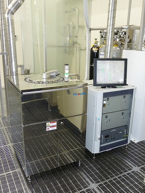
Specifications
・Sample types: SiO2, TiO2, Al2O3, Nb, others
・Sample size: 6-inch wafer-compatible
・Maximum film temperature range: 600℃, computerized
Characteristics
Capable of creating thin film via high-precision (angstrom order) film thickness control
Savannah 100 ALD film-forming system (Cambridge NanoTech)
Specifications
・Film formation materials: HfO2, Al2O3, ZrO2
・Maximum specimen size: φ 200 mm
Characteristics
Capable of realizing precise thickness via the accumulation of atomic layers one by one in a digitally controlled process and forming insulating film via the accumulation of thin Al2O3 and HfO2 film at formation temperatures of 100 to 250℃
Nanocarbon growth furnace, easy tube system (Nano Device)
Specifications
・Maximum substrate size: 2 × 2 cm
・Maximum growth temperature: 100℃
・Growth gases: methane, ethylene, argon, hydrogen, atmospheric pressure
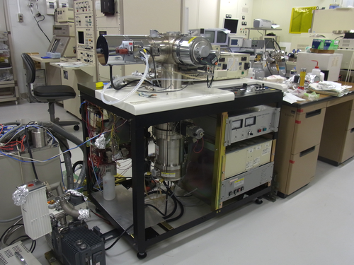
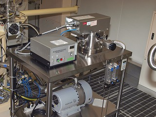
PAC-LMBE Compact Laser MB
Specifications
Light source: Excimer (KrF 248nm)
Specimen types:TiO2, SrTiO3
Maximum specimen size:2×2 cm
With a substrate heating system
Characteristics
RHEED allows you to monitor its film surface in situ
Etching technology
RIE-101iPH ICP high-density plasma etching system (Samco)
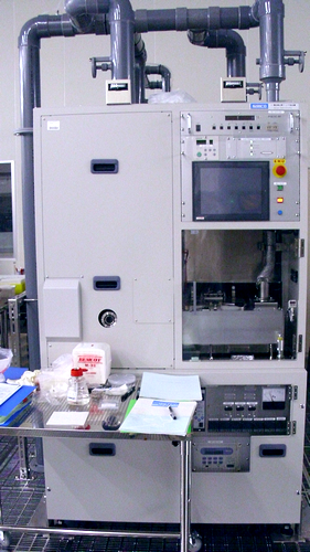
Specifications
・Gases used: SF6, C4F8, CF4, Ar, O2, CHF3, C3F8
・Maximum specimen size: 4 inches
Characteristics
Capable of high-precision etching on silicone, various types of thin metal film, compound semiconductors, and other materials
RIE-101iHS ICP high-density plasma etching system (Samco)
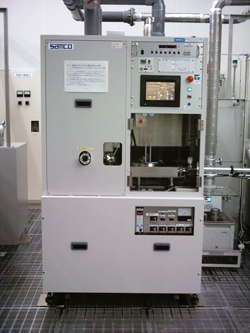
Specifications
・Gases used: Xe, Ar, O2, SiCl4, Cl2
・Maximum specimen size: 4 inches
Characteristics
Capable of high-precision etching on silicone, various types of thin metal film, compound semiconductors, and other materials
SPM-200 ICP dry etching system (Sumitomo Precision Products)
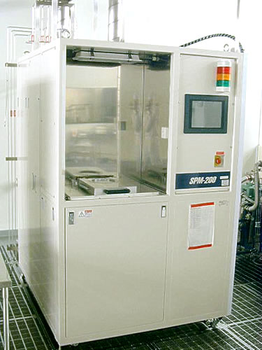
Specifications
・Gases used: SF6, C4F8, CF4, Ar, O2
・Maximum specimen size: 4 inches
Characteristics
Capable of high-precision etching mainly on silicone surfaces; Bosch-process compatible
EIS-700 ICP processor (Elionix)
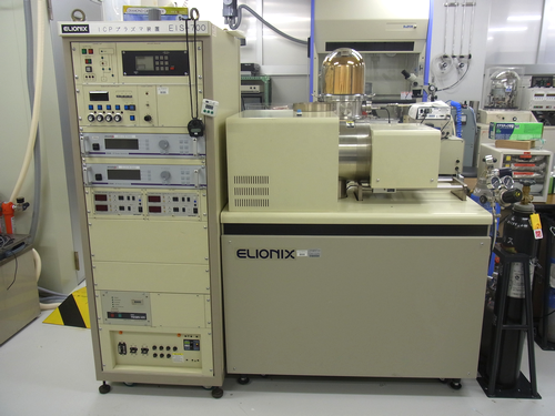
Specifications
・Gases used: CF4, O2, Ar
・Specimen size: 20 × 20 mm × 4
Characteristics
Dry etching system
NLD-500 Dry etching system (Ulvac)
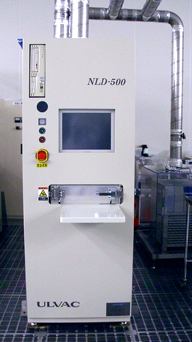
Specifications
・Gases used: CHF3, C3F8, SF6, C4F8, O2, Ar, He, N2, air
・Maximum specimen size: 4 inches
Characteristics
High-speed system using ICP plasma for etching mainly on oxidized materials. Capable of depth-direction control in nanometer order.
RIE-10NRV Reactive ion etching system (Samco)
Specifications
・Gases used: CF4, Ar, O2, CHF3
・Maximum specimen size: 8 inches
Characteristics
Capable of dry etching on SiO2/Si3N4Si insulating film
IBE-6000S Ion milling system (Ulvac)
Specifications
・Gas used: Ar
・Maximum specimen size: 4 inches Maximum thickness: 20 mm
Characteristics
For nanofabrication of metals and ceramics using Ar ion irradiation
EIS-200ER ECR processor (Elionix)
Specifications
・Ion gun: CR-type ion gun
・Ionized gases: Ar, O2, CF4, others
・Accelerating voltage: 100 to 3,000 V, continuously variable
・Maximum specimen size: 4 inches
Characteristics
Capable of etching, surface cleaning and other processes with less damage to substrates based on high current density even at an accelerating voltage. Also enables etching on insulators using neutralizing electrodes.
Evaluation technology
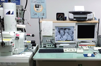
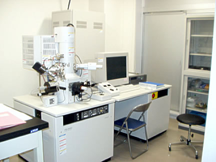
JSM-6700FT High-resolution field emission-type scanning electron microscope (JEOL)
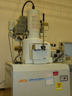
Specifications
・Accelerating voltage: 0.5 to 30 kV
・Magnifications: × 25 to 19,000 (LM mode),
×100 to 650,000 (SEM mode)
・Secondary electron resolution: 1.0 nm (at 15 kV), 2.2 nm (at 1 kV)
・With an EDS function and a two-point micro probe
Characteristics
Used to scan specimen surfaces with convergent electron beams and create images of emitted electrons. Also suitable for surface structural analysis.
M-500S Ellipsometer (JASCO)
Specifications
・Xe light source
・Measurement wavelength: 350 to 800 nm
・Horizontal specimen placement
Characteristics
Used to analyze thin film, surfaces and microstructures of materials by measuring relative phase changes of reflected polarization beams
Other processing technologies
EIP-3300 FIB processor (Elionix)
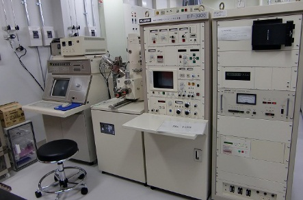
Specifications
・Ion acceleration power: 5 to 35 kV (Ga liquid metal ion source)
・Scanning magnification: × 100 to 80,000
・Element graphics: straight line (vertical, horizontal, oblique), rectangle, triangle, square, circle
・Capable of vector scanning and WCO deposition
Characteristics
Used to process specimens into optional shapes using a convergence ion beam
Other Open Facility Instruments
These are not part of the nano-technology platform instruments,
but inquiries and technical support are available.
SH-221 Environmental test device (Espec)
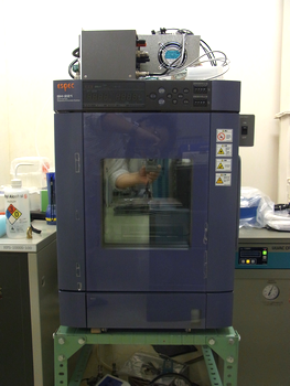
Specifications
・Source voltage: 13.5 A
・Temperature/humidity control system: balance temperature/humidity control (BTHC) system
・Temperature range: -20 to +150℃
・Humidity range: 30 to 95%
・Test area: W300 × H300 × D250 (mm)
Characteristics
With instrumentation enabling programmed operation of up to nine steps per pattern and setting of ascending and descending gradients of temperature/humidity. Besides fixed value setting, the device can also be used for temperature characteristic testing and temperature/humidity cycle testing.
KH-7700 Digital microscope (Hirox)
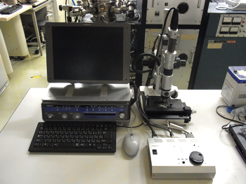
Specifications
・Imaging elements: 1/1.8-type 2,110,000-pixel CCD
・Scanning method: progressive
・Magnification: × 2,500
・3D profile/measurement/display
Characteristics
Capable of handling a wide range of processes from observation to data measurement, analysis, recording, management and output. Enable 2D and 3D tiling
WXS-156SL2, AM1.5GMM Solar cell evaluation system (Wacom)
Specifications
・Pursuant to JIS/IEC standards Class AAA
・ Emission intensity: 1 (sun)
・Maximum substrate size: 6 inches
Characteristics
Comprised of Solar sumilator, I-V measuring system, and Sample stage. The rays produced by the unit have a spectrum distribution that is quite similar to the natural solar spectrum. Capable of characteristic evaluation of PV cells or module.
PC-01-H Vacuum ultraviolet exposure system photo creator (N-Kobo)
Specifications
・Maximum specimen size: 1 inch
Characteristics
Capable of vacuum ultraviolet exposure and excimer ashing using an excimer lamp
Microstructure Characterization
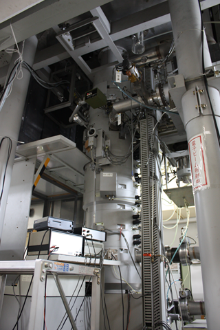
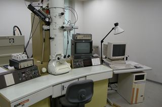
Ultrahigh-voltage electron microscope facility
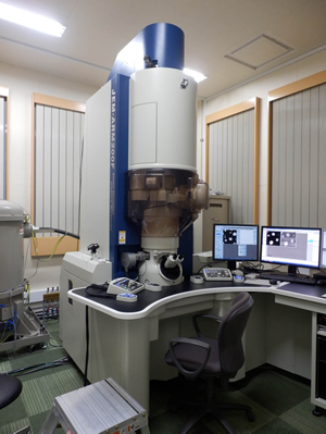
JEM-ARM-1300 Multi-beam ultrahigh-voltage electron microscope (JEOL)
Specifications
・Acceleration power: 400 to 1,300 kV
・Magnification: × 200 to 1,500,000
・Connection of two ion accelerators: 400 kV system, 300 kV system
・Particle resolution: 0.118 nm
・Other functions: specimen heating, cooling holder
Characteristics
Point resolution of 0.12 nm. Suitable for in-situ and 3D observation with electron beams capable of high specimen penetration. Simulates the damage processes of reactors and other materials by irradiating specimens with high-energy electron beams.
H-1300 Laser ultrahigh-voltage electron microscope (JEOL)
Specifications
・Acceleration power: up to 1,300 kV
・Particle resolution: 0.14 nm (top entry), 0.20 nm (side entry)
・Other functions: biaxial inclined heating, tension testing
Characteristics
Observation of thick film specimens, in-situ observation of specimen heating processes, processes of damage by electron beam irradiation and deformation behavior under stress
Electron microscopes
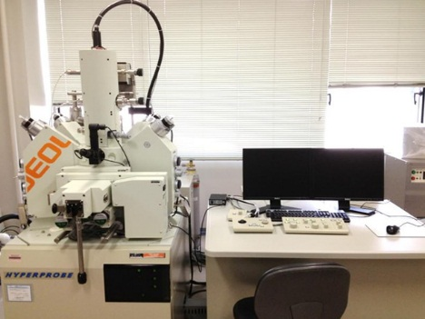
JSM-6500FA Field emission-type scanning electron microscope (JEOL)
Specifications
・Electron gun: Field emission-type (FE)
・Acceleration power: 0.5 to 30 kV
・Magnification: × 25 to 19,000
・Secondary electron resolution: 1.0 nm (15 kV), 2.2 nm (1 kV)
・Analysis functions: EDS (C to U), EBSD
・Specimen holder: max. 150 mm × 10 mm (H)
Characteristics
Used to scan specimen surfaces with convergent electron beams and create images of emitted electron. Also suitable for surface structural analysis.
Spin SEM (developed jointly by Eiko Engineering and Hokkaido University)
Specifications
・Blocking electrode-type spin analyzer
・Acceleration power: 30 kV
・10 to 60 keV ultrahigh vacuum/Ar sputter gun
・Substrate heating: 500℃
・RHEED with a spare heating chamber/metal deposition device
Characteristics
A spin-polarized scanning electron microscope (spin SEM) capable of detecting the secondary electron spin released when magnetic materials are irradiated with electron beams based on decomposition into three vector components (X, Y, Z). Supports spin quantitative analysis, magnetic imaging and other nano-scale processes.
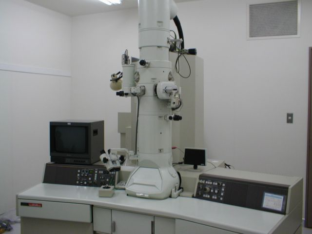
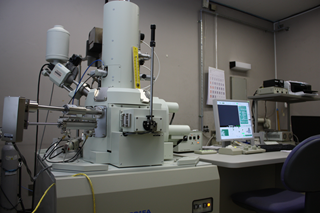
JEM-2010F Analysis TEM with a field emission-type electron gun (JEOL)
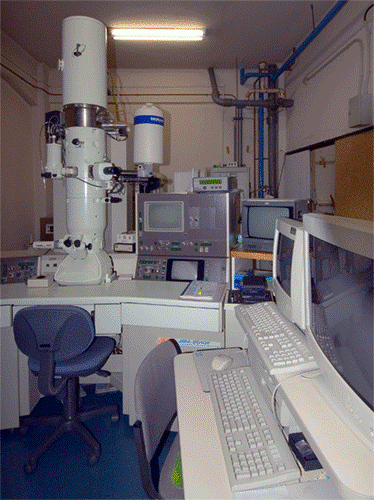
Specifications
・Acceleration power: 200 kV
・Particle resolution: 0.19 nm
・Analysis functions: EDS, EELS, GIF, STEM
・With a biaxial inclined analysis holder and a biaxial inclined heating holder
Characteristics
Transmission-type analyzer electron microscope with a field emission-type electron gun and diverse analyzers to support micro-composition/condition analysis of various materials
JEM-2010 (UHR) Electron microscope system for environmental cells (JEOL)
Specifications
・Acceleration power: 200 kV
・Magnification: × 1,000 to 1,500,000
・Analysis function: EDS
・With an environmental cell heating holder
Characteristics
Supports observation by imaging transmitted electrons.
HD-2000 Ultra-thin film evaluation system STEM (Hitachi High-Technologies)
Specifications
・Acceleration power: 200 kV
・Grid resolution: 0.24 nm
・Magnification: × 100 to 5,000,000
・Analysis functions: EDS, EELS
・SEM observation image: secondary electron observation, STEM observation, bright-field/dark-field images (z-contrast)
Characteristics
Supports Microstructure Characterization. Includes a bright-field/dark-field transmission electron detector and a secondary electron detector for observation and an energy dispersion-type characteristic x-ray detector for analysis.
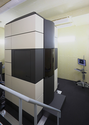
Ultrahigh-speed time-resolved photoelectron microscope system (TR-PEEM)
Specifications
・Spatial resolution: 8 nm or less
・Energy resolution: 150 meV or less
・Visual field range: 2 to 180 μm
・Time resolution: 7 fs or less
・Laser wavelength: 400 nm, 800 nm
・With a five-axial stage/sample heating mechanism
Characteristics
Supports time-resolved optical electron imaging with a combination of a femtosecond pulse laser and a photoelectron microscope (PEEM).
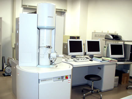
JEM-ARM200F Atomic Resolution Analytical Electron Microscope
Specifications
・Acceleration power:80kV, 200kV
・Analysis functions: EDS, EELS
Characteristics
With a STEM Cs corrector, the elemental analysis and mapping at the atomic resolution
becomes possible.
Titan Transmission Electron Microscope FEI
Specifications
・Acceleration power:60kV~300kV
・Analysis functions: EDS, ELLS, Tomography
Characteristics
With a S/Tem Cs corrector, XFEG gun
Biological microscopes
A1 High-speed laser confocal microscope for spectral imaging (Nikon)
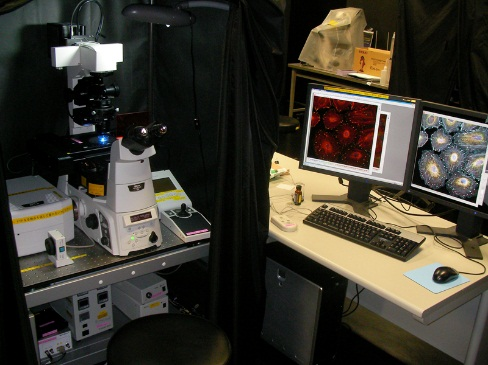
Specifications
・Scanning speed: 420 fps (512 × 16)/33 fps (512 × 512)
・Laser wavelength: 405 nm excitation light
・Suitable for spectral imaging; includes an auto-focus function.
Characteristics
A biological microscope supporting 3D structural and high-speed 4D (XYZ-T) observation of cells and tissues
Surface analyzers
JAMP-9500F Auger electron spectroscope (JEOL)
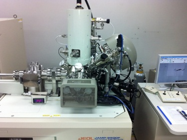
Specifications
・Acceleration power: 0.5 to 30 kV
・Magnification: × 25 to 500,000
・SEM spatial resolution: 3 nm
・Other analysis functions: EBSD, support for element analysis of Li or higher
Characteristics
Surface analyzer supporting depth-direction analysis using Ar ion sputtering and insulator analysis using a neutralizing electron gun
JPS-9200 X-ray photoelectron spectroscope (JEOL)
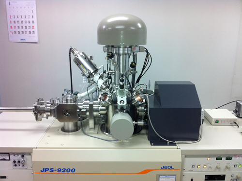
Specifications
・X-ray source anticathode: Al/Mg twin anode
・Acceleration power: 2 to 12 kV
・Resolution: 0.65 eV (monochrome x-ray source)
・Maximum load resistance: 500 W (Mg)/600 W (Al)
・Standard specimen: 10 × 10mm, 4 mm or less in thickness (max. 6 pieces)
・For large specimens: max. 90 mmφ, 1.5 mm or less in thickness
Characteristics
Used to analyze constituent elements and the chemical bond status of specimen surfaces based on X-ray irradiation
JXA-8530F Electron probe micro analyzer (FE-EPMA) (JEOL)
Specifications
・Acceleration power: 1 to 30 kV
・Scanning magnification: × 40 to 300,000
・Analysis functions: EDS, WDS
・Analysis element range: WDS: (Be) B to U, EDS: B to U
Characteristics
Supports 0.1 micron-order high-precision element analysis using an FE electron gun.
JAFM4500-LT Ultrahigh vacuum, ultralow temperature high-field SPM (JEOL)
Specifications
・Measurement modes: STM/NC-AFM, AFM, optical fiber interference mode
・Liquid He cryostat 4.2 K
・Vertical field: 8T Horizontal field: 2T
・Suitable for gradient magnetic field application
Characteristics
A scanning-type probe microscope capable of nano-scale measurement for specimen observation, mechanical, electric and various other properties
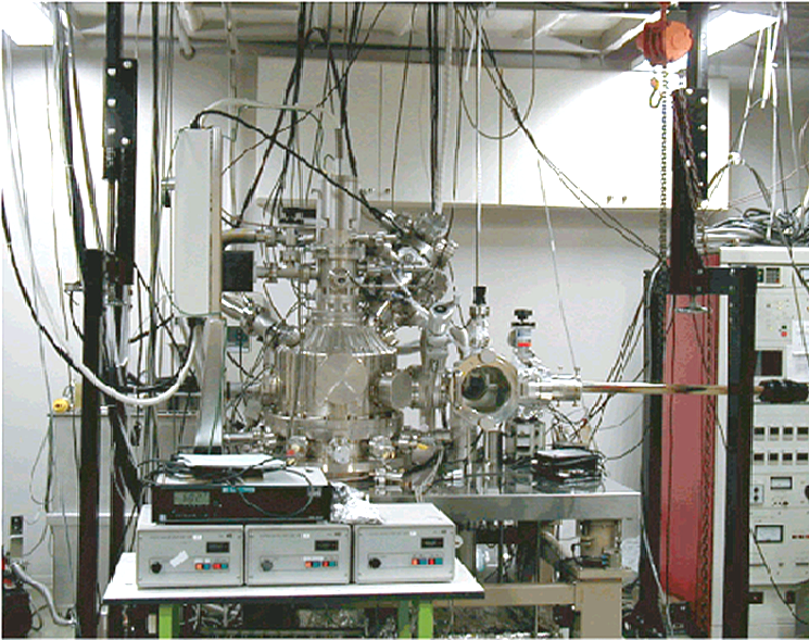
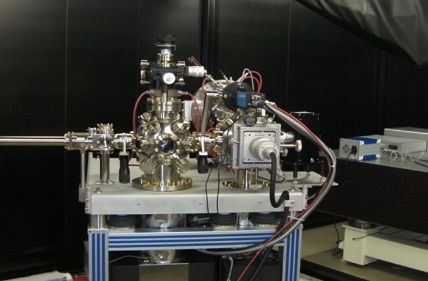
LT-STM/AFM Ultrahigh vacuum STM/spin-polarized STM system (VT-STM) (Omicron)
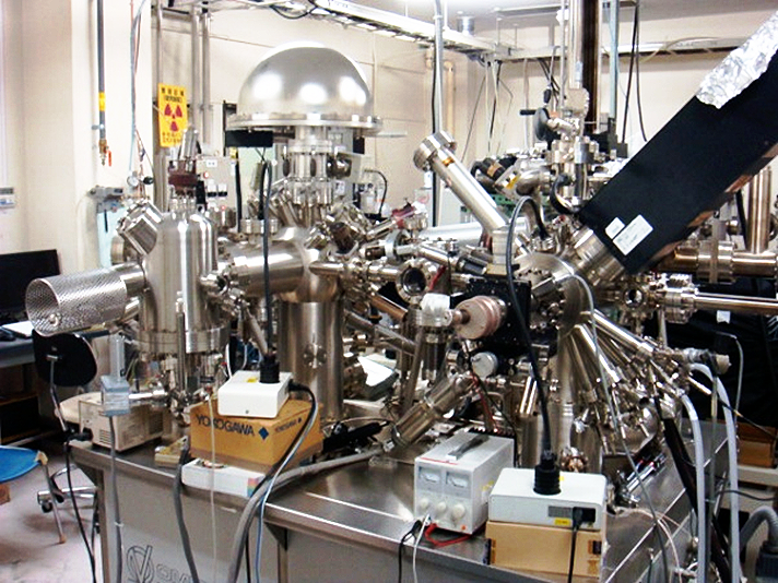
Specifications
・Probe-cleaning mechanism
・Spin-detectable probe-production mechanism
・Metallic epitaxy film mechanism
・RHEED, Ar sputter gun, FEM probe evaluation mechanism
・XPS, AES, LEED
・Specimen heating: 800℃; direct 1,200℃
・VT-STM: 20 K or less
Characteristics
A scanning electron microscope capable of detecting the secondary electron spin released when magnetic materials are irradiated with electron beams based on decomposition into three vector components (X, Y, Z). Supports spin quantitative analysis, magnetic imaging and other nano-scale processes.
Sample production devices
FIB FB-2100 Convergence ion beam processing/observation system (Hitachi High-Technologies)
Specifications
・Acceleration power: 10 to 40 kV
・Maximum magnification: × 280,000
・SIM resolution: 6.0 nm
・With a 3D holder/controller and a micro-sampling mechanism
Characteristics
For specimen nanofabrication using ion beams. Supports rough processing and finishing with variable acceleration power of 10 to 40 kV.
JIB-4600F/HKD FIB-SEM Combined beam processing/observation system (JEOL)
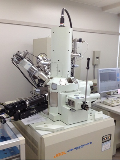
Specifications
・Acceleration power: 1 to 30 kV
・Magnification: × 20 to 1,000,000
・Image resolution: 5 nm (30 kV)
・Analysis functions: EDS, EBSD, 3D observation
Characteristics
Supports simultaneous FIB processing, EDS analysis, EBSD analysis, and high-resolution observation using FE-SEM
Other Open Facility Instruments
These are not part of the nano-technology platform instruments,
but inquiries and technical support are available.
JSM-7001FA Field emission-type scanning electron microscope (JEOL)
Specifications
・Electron gun: Field emission-type (FE)
・Acceleration power: 0.5 to 30 kV
・Magnification: × 10 to 80,000
・Secondary electron resolution: 1.2 nm (30 kV), 3.0 nm (1 kV)
・Analysis functions: EDS,EBSD
Characteristics
Supports nano-structural observation for surfaces and EDS/EBSD analysis from high-magnification observation while maintaining minimum aperture. Suitable for magnetic materials and various other specimens.
JEM-2000FX Analysis TEM with a field emission-type electron gun (JEOL)
Specifications
・Acceleration power: 200 kV
・Particle resolution: 0.28 nm
・Grid resolution; 0.20 nm
・Analysis function: EDS
Characteristics
Transmission-type analyzer electron microscope with a field emission-type electron gun and diverse analyzers to support micro-composition/condition analysis of various materials
Ion slicer (JEOL)
Specifications
・Acceleration power: 2 to 8 kV
Characteristics
Capable of producing sectional TEM specimens
Sample production devices
Specifications
・Cutting device
・Mechanical polishing device
・Electropolisher (Struers Tenupol-5)
・Ion polisher (Gatan PIPS)
・FIB processor (JEM-9320FIB)
・Pickup system
Characteristics
For production of electron microscope observation specimens