
Nanofabrication Platform Consortium
Hokkaido University provides support for nanofabrication in fields where nanotechnology can be used to accelerate advanced research, such as manufacturing of new nanodevices for light, electron and spin control, biotechnology and material development. It provides cutting-edge research, development support and technical consultation services by combining its high-precision processing devices and unique processing technology with the experience and enthusiasm of its researchers.
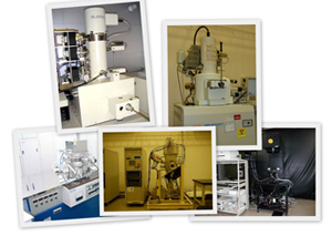
The university supports the creation of new technology and industry in Japan via two clean rooms on campus to produce optimal devices using combinations of equipment for lithography, film formation, etching and other work, as well as by fostering the development of human resources through equipment training courses and other opportunities. The project is run by the Office for the Promotion of Nanotechnology Collaborative Research under the Creative Research Institution (CRIS).
With the Center for Innovation and Business Promotion on its premises and the Business Spring area where public research institutes and venture businesses in Hokkaido gather, CRIS also has an environment ideal for active involvement in support for companies and other operators.
Microstructure Characterization Platform
Hokkaido University provides support for research on analysis/evaluation of materials and devices of nano- to micrometer-order in terms of (1) surface structure, (2) internal/3D structure and (3) electronic state analysis.
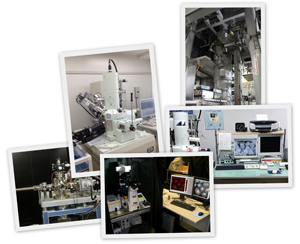
Research, technical and product development support is provided for the creation of new state-of-the-art function-added nanomaterials and the manufacture of new devices via the provision of systems for:
(1) surface structural analysis using state-of-the-art X-ray photoelectron and Auger electron spectroscopes, electron beam probe microanalyzers and other surface analyzers;
(2) internal/3D structural analysis conducted by combining diverse microscopes (including the world’s only ultrahigh-voltage electron microscope featuring two high-energy ion accelerators) with SEM-FIB and other sample processing devices, and;
(3) analysis in controlled environments using in-situ TEM observation with an environmental cell holder and ultrahigh-vacuum, ultralow-temperature and high-field SPM, and analysis of electronic states and real-time kinetics of nanodevices using an ultrahigh-speed time-resolved photoemission electron microscopes, a high-speed spectral imaging laser confocal microscope and other devices.